How Single Wafer Tracking Optimizes Solar Cell Production
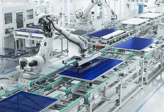
Manufacturers who want to produce solar cells with maximum efficiency must make the best use of modern cell architectures, high performance production machines and software for production control. The quality of solar cells, however, can only be measured at the end of the manufacturing process. The traceability of deviations from data collected during the process is therefore of crucial importance for root cause research and quality optimization. That is where the range of functions of the Manufacturing Execution System (MES) plays an important role. Single wafer tracking in particular provides measurable advantages as an extension of product data acquisition. This specialized form of end-to-end process transparency enables process engineers to significantly reduce costs by shortening the ramp-up phase. The product data in the MES is then used to continuously optimize product quality and process stability. In this blog article, you will find out more about how single wafer tracking works, and how it benefits the photovoltaic industry.
Single Wafer Tracking – What Is It?
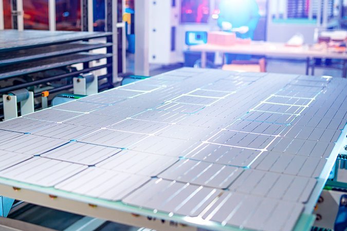
Single wafer tracking refers to the cross-process tracking and monitoring of the manufacturing process of solar cells at wafer level. This involves tracking individual wafers on their way through production and linking them to process data. While physical single wafer tracking requires markings such as QR codes on the wafers, virtual single wafer tracking does not require these markings, as only transport and process carriers must be uniquely identifiable, e.g. via RFID.
Comparison between Virtual and Physical Tracking
How physical tracking works
Physical tracking of materials or products requires markings that enable unique identification. These markings usually consist of a product ID, which is applied as a QR code, barcode or as an RFID chip at the start of the production process. This product ID is documented as an identifier in the MES system and linked to the process data. Within the production line, e.g. when loading a production machine, this marking is recorded and transmitted to the MES together with new process data. Simpler forms of physical tracking combine multiple products into one batch, which can be identified by a shared batch ID.
The challenges of physical tracking
- Markings on wafers can impair cell quality because they affect the active surface, for example if a laser is used.
- The legibility of markings often fluctuates during surface treatment processes such as etching or coating and can have a negative impact on the tracking rate.
- Physical tracking involves high investment costs for marking lasers and reading devices (e.g. cameras) at every stage of the process.
- The level of detail in physical tracking of a wafer is limited to when the wafers enter and exit a process. Within the processes, there is no further position recording and tracking by the process machine.
- Solar cells are often manufactured using carriers or trays in which several wafers are processed simultaneously. Because the position of a wafer in carriers and trays has an impact on their quality, end-to-end tracking of each wafer is relevant for process optimization.
How single wafer virtual tracking works
Virtual tracking is based on a combination of carrier tracking, tracking information from process machines and a full tracking history in the MES. Products are tracked along the production line based on position or carrier changes and linked to process data. The MES records and orchestrates all carrier and product movements. In actual fact, it is an extension of physical tracking with more detail, because the carriers are identified physically, e.g. using RFID, and the tracking history is then updated in the MES. An increased tracking rate improves the data situation and statistics, which serve as the basis for quality management and is the starting point for optimizing process stability and quality.
The challenges of virtual tracking
- Machine PLCs need to have an interface to send virtual tracking information to the MES.
- Changes in the position of the individual wafers due to the processes must be tracked by the machine, which also includes carrier changes.
- The machine must detect the removal of individual wafers or wafer breakages in order to avoid tracking losses.
Virtual and Physical Single Wafer Tracking in FabEagle®MES for Data Correlation and Evaluation
Our FabEagle®MES supports both physical and virtual single wafer tracking to provide the largest possible database for optimization. The tracking and evaluation of this data in the FabEagle®MES enables precise analysis and optimization of manufacturing processes. In particular, the integrated functions for correlating various data sets and reporting statistical variables play a decisive role here.
An important function of our MES is the tracking and provision of wafer data. By recording position data and process values, for example, a heat map can be generated which enables a visualization of cell efficiency as a function of the position of the wafers in the carriers and process chambers. This heat map provides a clear overview of the distribution of product quality within the process chamber and helps to identify and optimize potential weak points in the process. By recording position and time information for each wafer, it is also possible to analyze the influence of different process routes. This detailed analysis makes it possible to understand the influence of process parameters over the entire production process and to optimize them in a targeted manner.
Correlating data is another important task of the MES. Relations between various parameters can be identified by combining data from the cell tester at the end of production with process, quality and recipe data. This enables targeted analysis and optimization of manufacturing processes. In addition, image data from electroluminescence imaging (EL imaging) can also be included in the analysis so that optical and electrical quality control can be carried out and potential defects identified at an early stage.
Another important tool in the MES is statistical process control (SPC). This enables continuous monitoring of process stability and quality by identifying deviations from the target values at an early stage and taking appropriate measures. By analyzing trend data, long-term developments and tendencies can also be identified, which serve as a basis for future decisions and optimizations.
Outlook for Data Acquisition and Evaluation
Machine learning for automatic data evaluation: Applying machine learning to the MES database enables precise analysis of large volumes of data sets in order to identify dependencies and trends in production processes. On this basis, processes can then be optimized.
Efficient data storage and management in a data lake: Implementing data lakes makes it easier to centrally store and access data in various formats as well as data sources outside the MES over extended periods of time.
Hybrid tracking solutions for precise process tracking: The combination of virtual and physical tracking enables precise monitoring of production processes using various technologies.
Application in other industries such as circuit board manufacturing: Single wafer tracking in the MES can also be used in other industries, such as circuit board manufacturing, to optimize processes and improve product quality.
Conclusion: Optimizing Solar Cell Production Using Single Wafer Tracking
A Manufacturing Execution System specializing in single wafer tracking plays a decisive role in optimizing solar cell production. By precisely tracking and monitoring each individual wafer throughout the manufacturing process, manufacturers can quickly and comprehensibly improve cell efficiency and product quality. The advantages of this technology are
- reducing costs by shortening the ramp-up phase,
- continuous monitoring and optimization of processes, and
- improving data and statistics for quality management.
Using machine learning for automatic data evaluation, efficient data storage and management with data lake architectures, hybrid tracking solutions, and applying the technology in other industries such as circuit board manufacturing are promising developments for the future. These technologies offer further potential to increase efficiency and quality in the manufacturing industry and help manufacturers meet constantly increasing specifications.

Want to Learn More about Single Wafer Tracking? I Will Be Happy to Help You!